CREE C2M0080120D
| Line 8: | Line 8: | ||
=== Static === | === Static === | ||
| − | Fig. 1 reports the comparison between the experimental DC Transfer curves and the simulated static output characteristics at different junction temperature values. It can be observed as the current capabilty of the MOSFET increases for higher temperatures when the gate voltage is low (NTC: negative temperature coefficient), while it decreases when Vgs is high (PTC: positive temperature coefficient) | + | Fig. 1 reports the comparison between the experimental DC Transfer curves and the simulated static output characteristics at different junction temperature values. It can be observed as the current capabilty of the MOSFET increases for higher temperatures when the gate voltage is low (NTC: negative temperature coefficient), while it decreases when Vgs is high (PTC: positive temperature coefficient). |
{| style="margin: 0 auto;" | {| style="margin: 0 auto;" | ||
| Line 15: | Line 15: | ||
|- | |- | ||
|} | |} | ||
| + | Fig. 2 reports the comparison between the experimental DC Output curves and the simulated static characteristics at different junction temperature values. | ||
{| style="margin: 0 auto;" | {| style="margin: 0 auto;" | ||
|- | |- | ||
| [[File:C2M0080120D ID VDS.png|link=|thumb|400px|Fig. 2. DC Output Characteristics.]] | | [[File:C2M0080120D ID VDS.png|link=|thumb|400px|Fig. 2. DC Output Characteristics.]] | ||
| + | |- | ||
| + | |} | ||
| + | Fig. 3 reports the comparison between the experimental capacitance measurements for a drain bias sweep (Vgs=0) and the simulated curves. | ||
| + | {| style="margin: 0 auto;" | ||
| + | |- | ||
| + | | [[File:C2M0080120D cap.png|link=|thumb|400px|Fig. 2. DC Output Characteristics.]] | ||
| + | |- | ||
| + | |} | ||
| + | Fig. 3 reports the comparison between the measured conduction power losses and the simulated ones for increasing drain current and different junction temperatures. | ||
| + | {| style="margin: 0 auto;" | ||
| + | |- | ||
| + | | [[File:C2M0080120D condloss.png|link=|thumb|400px|Fig. 2. DC Output Characteristics.]] | ||
|- | |- | ||
|} | |} | ||
Revision as of 16:05, 22 November 2016
Contents |
Download
Identification tool
The parameter extraction has been done by means of a Matlab-PSpice parameter identification tool for SiC MOSFETs called MOSPEX which you can find here. It is a user-friendly Graphic User Interface (GUI) that you can use on your own.
Tests performed
Static
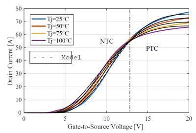
Fig. 1 reports the comparison between the experimental DC Transfer curves and the simulated static output characteristics at different junction temperature values. It can be observed as the current capabilty of the MOSFET increases for higher temperatures when the gate voltage is low (NTC: negative temperature coefficient), while it decreases when Vgs is high (PTC: positive temperature coefficient).
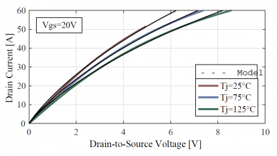
Fig. 2 reports the comparison between the experimental DC Output curves and the simulated static characteristics at different junction temperature values.
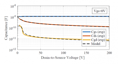
Fig. 3 reports the comparison between the experimental capacitance measurements for a drain bias sweep (Vgs=0) and the simulated curves.
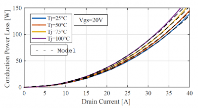
Fig. 3 reports the comparison between the measured conduction power losses and the simulated ones for increasing drain current and different junction temperatures.
Dynamic
Fig. 2 (a) shows the comparison between measured and simulated turn-off waveforms at the following testing conditions: IC=560 A, VDC=900V and T=25C. The comparison between the PSpice simulation and experimental results validating the temperature-dependent IGBT model under inductive switching conditions are shown in Figs. 2(b) and 2(c) at 75ºC and 125ºC, respectively. Fig. 2 (d) shows the comparison between the experimental curves at different current and voltage levels (IC=670 A, VDC=1100V).


